HPC
NVIDIA H100 - Newest Data Center GPU built on Hopper Architecture
March 24, 2023
9 min read

Exxact Corporation now offers solutions featuring the new NVIDIA H100 Tensor Core GPU, and in this blog, we’ll examine what makes it such a powerful enterprise accelerator.
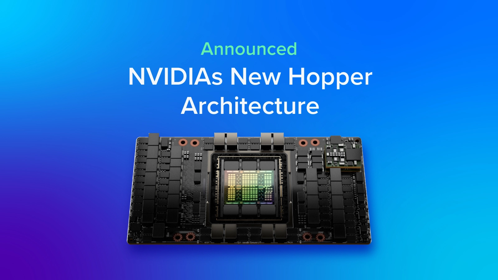
During the GTC 2022 Spring keynote, NVIDIA CEO and founder Jensen Huang announced the anticipated next generation of AI computing. Built on the new NVIDIA Hopper™ architecture, the NVIDIA H100 is taking the reins as the company’s next flagship GPU.
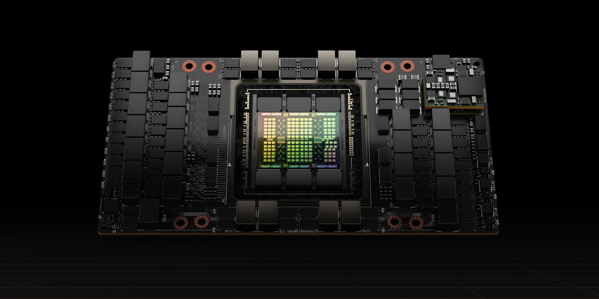
| GPU Features | NVIDIA H100 SXM5 | NVIDIA H100 PCIe | NVIDIA H100 NVL* |
| GPU Architecture | Hopper | Hopper | Hopper |
| Form Factor | SXM5 | PCIe 5.0 | 2x PCIe 5.0 |
| Cores | 16896 | 14592 | 2x 16896 |
| Tensor Cores | 528 | 456 | 528 |
| GPU Boost Clock | 1.98 GHz | 1.76 GHz | TBA |
| Memory Interface | 5120-bit | 5120-bit | 2x 5120-bit |
| GPU Memory | 80 GB HBM3 | 80 GB HBM2e | 2x 94 GB HBM3 |
| GPU Memory Bandwidth | 3.35 TB/s | 2 TB/s | 7.8 TB/s |
| L2 Cache Size | 50 MB | 50 MB | 2x 50MB |
| Max TDP | Up to 700W (configurable) | Up to 350W (configurable) | 2x 350-400W (configurable) |
| Transistors | 80 billion | 80 billion | 80 Billion |
| GPU Die Size | 814 mm2 | 814 mm2 | 814 mm2 |
| TSMC Manufacturing Process | 4N customized for NVIDIA | 4N customized for NVIDIA | 4N customized for NVIDIA |
*3-24-2023: Added preliminary specifications for NVIDIA H100 NVL
Tensor Cores in NVIDIA GPUs handle the matrix multiplication and accumulate in math operations to provide exceptional AI and HPC performance. These cores operate in parallel across SMs to deliver massive increases in throughput and efficiency first introduce in the NVIDIA V100. 4th Generation Tensor Cores in H100 deliver double the throughput in matrix multiplication compared to the A100, theoretically even higher with regards to higher boost clocks. H100 can perform these calculations faster while saving up to 30% operand delivery power
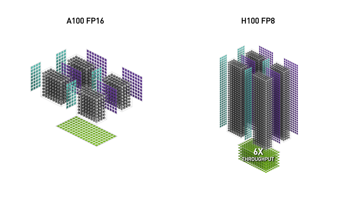
In addition to the advancement in Tensor Core technology, H100 can train on a new tensor processing format FP8. FP8 supports computations requiring less dynamic range with more precision halving the storage requirement while doubling throughput compared to FP16. To increase precision dramatically, NVIDIA H100 incorporates a new Transformer Engine that uses executes using dynamic mixed precision processing on both FP8 and FP16 numerical formats to reduce usage on data usage and increase speeds while retaining precision and accuracy.
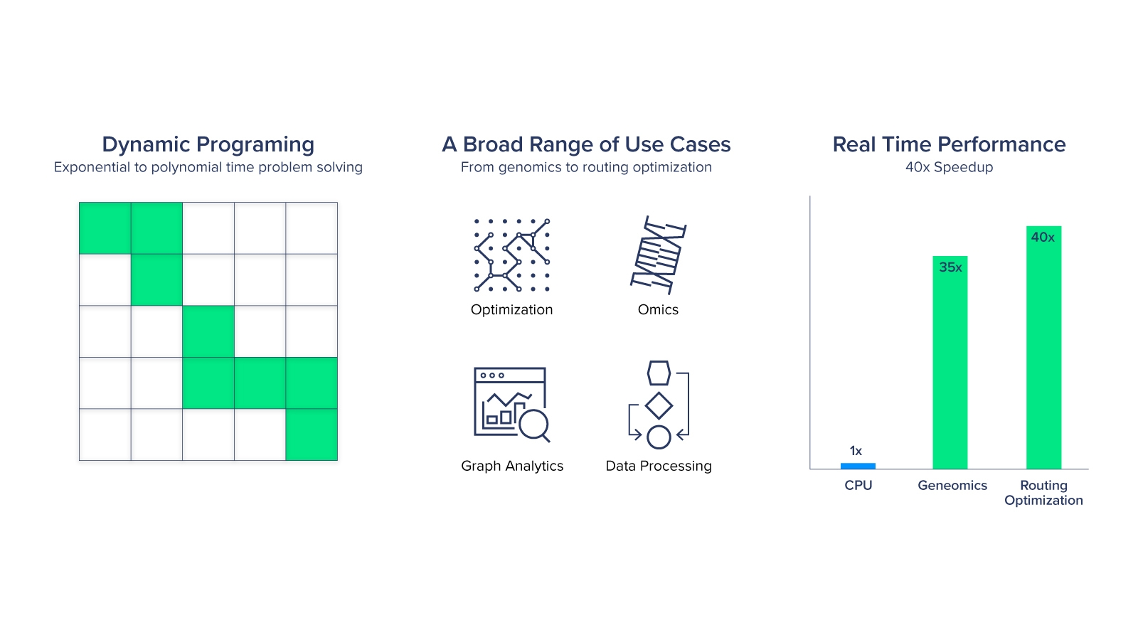
By introducing new DPX Instructions to accelerate dynamic programming algorithms, the H100 can perform 7x faster than the last generation Ampere. Dynamic programming (DP) is an algorithmic technique for solving a complex recursive problem by breaking it down into simpler sub-problems. By storing the results of sub-problems, DP algorithms reduce computational complexity. These new instructions provide faster times-to-solutions for problems such as disease diagnosis, route optimization, graph analytics, and more. The H100 is perfect for data analytics just as much as it is perfect for AI acceleration.
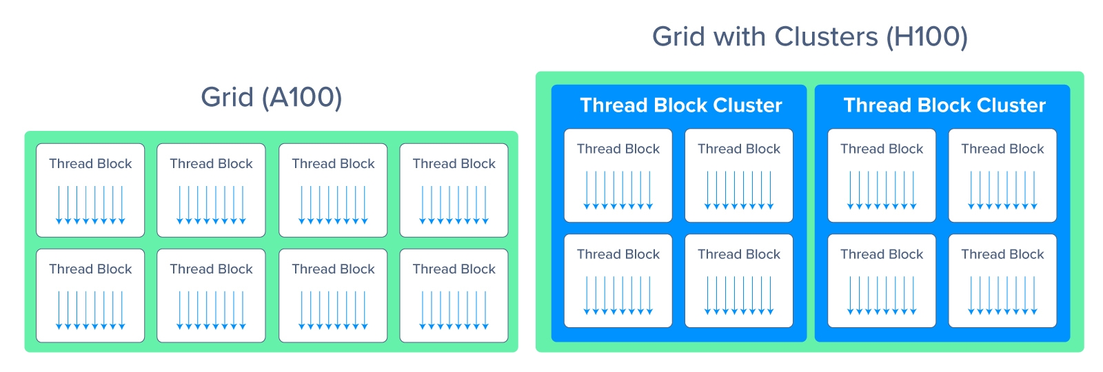
The complexity of NVIDIA H100 needs a new way to organize and control the locality of thread blocks. Thread block contains concurrent threads on an SM; to further organize, the hierarchical addition of thread block clusters increases the efficiency of concurrent threads over the entire SM. This grouping has also enabled distributed shared memory (DSMEM) to enable efficient data exchange using an SM-to-SM network instead of a global memory network. Thread Block Clusters and DSMEM accelerated data exchanged by about 7x.
HBM stands for high bandwidth memory, a different format of memory interface than we are used to (GDDR). HBM memory is reserved for data center usage since it is not typically used to display graphics but instead used for performance-thirsty tasks like AI and advanced computing, exactly what the H100 was intended for!
NVIDIA H100 SXM5 model comes equipped with HBM3 memory with about 3TB/s bandwidth, a 2x increase over A100. The H100 PCIe will come equipped with HBM2e running at 2TB/s still outperforming the A100’s HBM2 memory interface by about 1.5x.
The cache size has also increased in the H100 with a 50MB size. Larger caches can store larger amounts of data to reduce the number of trips back to memory. Keeping memory onboard the die means a shorter distance and less time to fetch data. Both the SXM and PCIe versions of H100’s DRAM and L2 cache enable sub-system support data compression and decompression technology to optimize usage and performance.
The new H100 GPU chip means there's a new NVIDIA DGX™. NVIDIA announces the DGX H100, which has 8 NVIDIA H100 SXM5s connected via 4 3rd Generation NVLink Switch Chips. NVSwitch provides links to pairs of GPUs to accelerate multi-GPU interconnectivity of 900 GB/s and 3.6 TB/s of total throughput providing hardware acceleration with multicast and NVIDIA SHARP in-network reductions.
The DGX H100 has 640 Billion Transistors, 32 petaFLOPS of AI performance, 640 GBs of HBM3 memory, and 24 TB/s of memory bandwidth. The DGX H100 is the smallest form of a unit of computing for AI. DGX can be scaled to DGX PODS of 32 DGX H100s linked together with NVIDIA’s new NVLink Switch System powered by 2 NVSwitches.
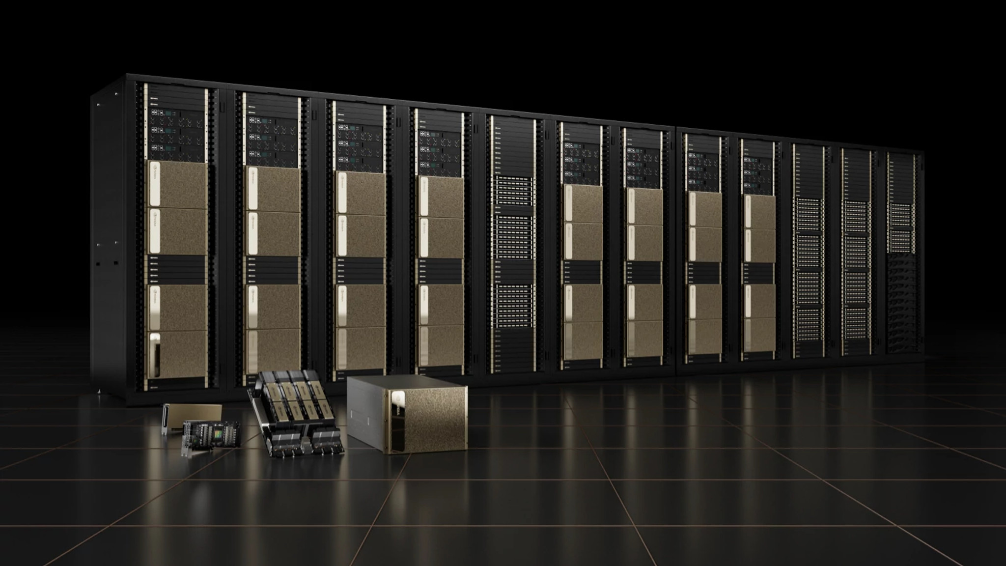
Image: NVIDIA
Before the NVLink Switch System, Mellanox LinkX Optic InfiniBand was a fast and low-cost way to create high speeds but adopted a leaf and spine architecture where data had to cross 2 mediums. The NVLink Switch System instead directly connects nodes through a single rack of 32 units of NVLink Switch system connected in a 2 H100s to 1 NVLink tapered, fat tree topology enabling a total of 256 H100 GPUs to be connected over NVLink. The NVIDIA DGX H100 SuperPod™ has 20.5 TB of HMB3 Memory and a staggering 57.6 TB/s of all-to-all bandwidth. The NVLink Switch System effectively multiplies bisectional bandwidth between the GPUS by 9x making it possible to accelerate even the most significant AI jobs multitudes faster. With 1 exaFLOPS of AI performance and 192 teraFLOPS of SHARP in-network compute the DGX H100 SuperPOD blows any supercomputer of today out of the water.
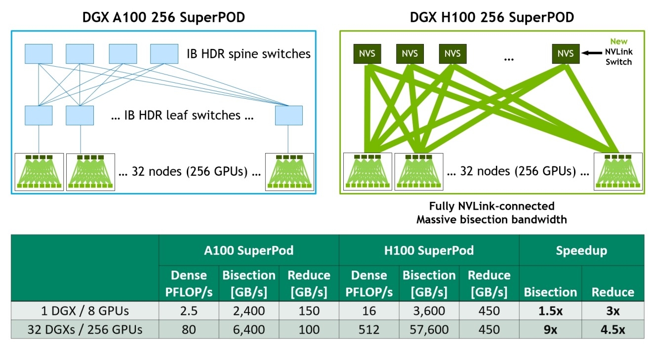
Image: NVIDIA
A single NVLink Switch System node can handle a max of 32 DGX H100s. Multiple DGX Pods connect with the new Quantum 2 Infiniband Switch with SHARP in-networking computing, performance isolation, and congestion control to scale to thousands of H100 GPUs. NVIDIA is demonstrating its advancement in both AI and networking to build Eos, the first Hopper AI factory containing 576 DGX H100 or 4608 H100 GPUs. This infrastructure is estimated to hit 275 petaFLOPS of scientific computing and 18 exaFLOPS of AI processing expected to be the world's fastest computer.
We expect a lot of innovation to trickle down NVIDIA’s AI and HPC product lines, with such a significant generational leap with its latest GPU architecture. The NVIDIA Hopper architecture has already brought a Transformer Engine to the new NVIDIA Ada Lovelace architecture as well as a strong emphasis on AI computing through the massive addition of Tensor Cores to the GeForce RTX GPUs.
A five-year license for the NVIDIA AI Enterprise software suite is now included with mainstream servers featuring the H100 Tensor Core GPU. NVIDIA AI Enterprise is an end-to-end program suite of AI and data analytics software enabling any business to leverage the power of AI.
With industry-leading AI developers, NVIDIA offers unparalleled support for developing AI models. This optimizes the development and deployment of AI workflows and ensures organizations have access to the AI frameworks and tools needed to build AI chatbots, recommendation engines, vision AI applications, and more. The possibilities of AI are limitless and only bound by what we instruct our machines to learn.
NVIDIA H100 systems are now available for order! NVIDIA partner systems with HGX H100 will begin shipping starting October 2022. NVIDIA DGX H100 can be ordered for delivery in Q1 2023.
Have questions about the NVIDIA H100 GPU, or how to upgrade your current infrastructure?
Contact Exxact today
Exxact Corporation now offers solutions featuring the new NVIDIA H100 Tensor Core GPU, and in this blog, we’ll examine what makes it such a powerful enterprise accelerator.
During the GTC 2022 Spring keynote, NVIDIA CEO and founder Jensen Huang announced the anticipated next generation of AI computing. Built on the new NVIDIA Hopper™ architecture, the NVIDIA H100 is taking the reins as the company’s next flagship GPU.
| GPU Features | NVIDIA H100 SXM5 | NVIDIA H100 PCIe | NVIDIA H100 NVL* |
| GPU Architecture | Hopper | Hopper | Hopper |
| Form Factor | SXM5 | PCIe 5.0 | 2x PCIe 5.0 |
| Cores | 16896 | 14592 | 2x 16896 |
| Tensor Cores | 528 | 456 | 528 |
| GPU Boost Clock | 1.98 GHz | 1.76 GHz | TBA |
| Memory Interface | 5120-bit | 5120-bit | 2x 5120-bit |
| GPU Memory | 80 GB HBM3 | 80 GB HBM2e | 2x 94 GB HBM3 |
| GPU Memory Bandwidth | 3.35 TB/s | 2 TB/s | 7.8 TB/s |
| L2 Cache Size | 50 MB | 50 MB | 2x 50MB |
| Max TDP | Up to 700W (configurable) | Up to 350W (configurable) | 2x 350-400W (configurable) |
| Transistors | 80 billion | 80 billion | 80 Billion |
| GPU Die Size | 814 mm2 | 814 mm2 | 814 mm2 |
| TSMC Manufacturing Process | 4N customized for NVIDIA | 4N customized for NVIDIA | 4N customized for NVIDIA |
*3-24-2023: Added preliminary specifications for NVIDIA H100 NVL
Tensor Cores in NVIDIA GPUs handle the matrix multiplication and accumulate in math operations to provide exceptional AI and HPC performance. These cores operate in parallel across SMs to deliver massive increases in throughput and efficiency first introduce in the NVIDIA V100. 4th Generation Tensor Cores in H100 deliver double the throughput in matrix multiplication compared to the A100, theoretically even higher with regards to higher boost clocks. H100 can perform these calculations faster while saving up to 30% operand delivery power
In addition to the advancement in Tensor Core technology, H100 can train on a new tensor processing format FP8. FP8 supports computations requiring less dynamic range with more precision halving the storage requirement while doubling throughput compared to FP16. To increase precision dramatically, NVIDIA H100 incorporates a new Transformer Engine that uses executes using dynamic mixed precision processing on both FP8 and FP16 numerical formats to reduce usage on data usage and increase speeds while retaining precision and accuracy.
By introducing new DPX Instructions to accelerate dynamic programming algorithms, the H100 can perform 7x faster than the last generation Ampere. Dynamic programming (DP) is an algorithmic technique for solving a complex recursive problem by breaking it down into simpler sub-problems. By storing the results of sub-problems, DP algorithms reduce computational complexity. These new instructions provide faster times-to-solutions for problems such as disease diagnosis, route optimization, graph analytics, and more. The H100 is perfect for data analytics just as much as it is perfect for AI acceleration.
The complexity of NVIDIA H100 needs a new way to organize and control the locality of thread blocks. Thread block contains concurrent threads on an SM; to further organize, the hierarchical addition of thread block clusters increases the efficiency of concurrent threads over the entire SM. This grouping has also enabled distributed shared memory (DSMEM) to enable efficient data exchange using an SM-to-SM network instead of a global memory network. Thread Block Clusters and DSMEM accelerated data exchanged by about 7x.
HBM stands for high bandwidth memory, a different format of memory interface than we are used to (GDDR). HBM memory is reserved for data center usage since it is not typically used to display graphics but instead used for performance-thirsty tasks like AI and advanced computing, exactly what the H100 was intended for!
NVIDIA H100 SXM5 model comes equipped with HBM3 memory with about 3TB/s bandwidth, a 2x increase over A100. The H100 PCIe will come equipped with HBM2e running at 2TB/s still outperforming the A100’s HBM2 memory interface by about 1.5x.
The cache size has also increased in the H100 with a 50MB size. Larger caches can store larger amounts of data to reduce the number of trips back to memory. Keeping memory onboard the die means a shorter distance and less time to fetch data. Both the SXM and PCIe versions of H100’s DRAM and L2 cache enable sub-system support data compression and decompression technology to optimize usage and performance.
The new H100 GPU chip means there's a new NVIDIA DGX™. NVIDIA announces the DGX H100, which has 8 NVIDIA H100 SXM5s connected via 4 3rd Generation NVLink Switch Chips. NVSwitch provides links to pairs of GPUs to accelerate multi-GPU interconnectivity of 900 GB/s and 3.6 TB/s of total throughput providing hardware acceleration with multicast and NVIDIA SHARP in-network reductions.
The DGX H100 has 640 Billion Transistors, 32 petaFLOPS of AI performance, 640 GBs of HBM3 memory, and 24 TB/s of memory bandwidth. The DGX H100 is the smallest form of a unit of computing for AI. DGX can be scaled to DGX PODS of 32 DGX H100s linked together with NVIDIA’s new NVLink Switch System powered by 2 NVSwitches.
Image: NVIDIA
Before the NVLink Switch System, Mellanox LinkX Optic InfiniBand was a fast and low-cost way to create high speeds but adopted a leaf and spine architecture where data had to cross 2 mediums. The NVLink Switch System instead directly connects nodes through a single rack of 32 units of NVLink Switch system connected in a 2 H100s to 1 NVLink tapered, fat tree topology enabling a total of 256 H100 GPUs to be connected over NVLink. The NVIDIA DGX H100 SuperPod™ has 20.5 TB of HMB3 Memory and a staggering 57.6 TB/s of all-to-all bandwidth. The NVLink Switch System effectively multiplies bisectional bandwidth between the GPUS by 9x making it possible to accelerate even the most significant AI jobs multitudes faster. With 1 exaFLOPS of AI performance and 192 teraFLOPS of SHARP in-network compute the DGX H100 SuperPOD blows any supercomputer of today out of the water.
Image: NVIDIA
A single NVLink Switch System node can handle a max of 32 DGX H100s. Multiple DGX Pods connect with the new Quantum 2 Infiniband Switch with SHARP in-networking computing, performance isolation, and congestion control to scale to thousands of H100 GPUs. NVIDIA is demonstrating its advancement in both AI and networking to build Eos, the first Hopper AI factory containing 576 DGX H100 or 4608 H100 GPUs. This infrastructure is estimated to hit 275 petaFLOPS of scientific computing and 18 exaFLOPS of AI processing expected to be the world's fastest computer.
We expect a lot of innovation to trickle down NVIDIA’s AI and HPC product lines, with such a significant generational leap with its latest GPU architecture. The NVIDIA Hopper architecture has already brought a Transformer Engine to the new NVIDIA Ada Lovelace architecture as well as a strong emphasis on AI computing through the massive addition of Tensor Cores to the GeForce RTX GPUs.
A five-year license for the NVIDIA AI Enterprise software suite is now included with mainstream servers featuring the H100 Tensor Core GPU. NVIDIA AI Enterprise is an end-to-end program suite of AI and data analytics software enabling any business to leverage the power of AI.
With industry-leading AI developers, NVIDIA offers unparalleled support for developing AI models. This optimizes the development and deployment of AI workflows and ensures organizations have access to the AI frameworks and tools needed to build AI chatbots, recommendation engines, vision AI applications, and more. The possibilities of AI are limitless and only bound by what we instruct our machines to learn.
NVIDIA H100 systems are now available for order! NVIDIA partner systems with HGX H100 will begin shipping starting October 2022. NVIDIA DGX H100 can be ordered for delivery in Q1 2023.
Have questions about the NVIDIA H100 GPU, or how to upgrade your current infrastructure?
Contact Exxact today
