HPC
What is a CPU Die Shrink and What Does it Mean for the Future?
July 27, 2017
5 min read


Central processing units (CPUs) are constantly becoming smaller and denser, resulting in more power and efficiency. Ever since Intel's first Pentium CPU was released using a 0.8 micrometer (μm) manufacturing process, CPUs have drastically decreased in overall size. Fractions of a micrometer were the standard die size for a decade. Then with the release of the second iteration of the Intel Pentium III processor, the switch was made to nanometer (nm), which is 1/1000 the size of a micrometer. The processor itself ended up using a mere 180 nm die shrink.
The term die shrink, also called optical shrink or process shrink, refers to semiconductor scaling of semiconductor devices, specifically transistors. "Shrinking a die" is to create an identical circuit using advanced fabrication processes that typically involve an advance lithographic node. Since the release of the Intel Pentium III processor, nanometers continues to be the current size for any and all CPU transistors.
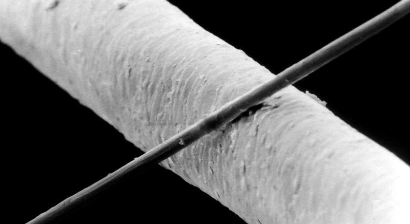
To provide a concrete example, we'll compare CPU transistors to a human hair strand using the above image. The thicker strand in the image is a piece of human hair and the smaller strand is 6 μm carbon filament. We mentioned previously that Intel's first Pentium processor utilized 0.8 μm transistors, which is smaller than the 6 μm carbon filament and is considered large in today's CPU microarchitecture standards. The current mainstream standard offered by both Intel and AMD is 14 nanometers (nm). Remember, one nanometer is 1/1000 the size of a micrometer, making it substantially smaller than the carbon filament. Intel's 14 nm microarchitecture is called Kaby Lake and includes the "7th Gen" 7000 series of processors. Kaby Lake was originally meant to be a die shrink, but due to the growing amount of hurdles that comes with dealing with continually decreasing sizes, Kaby Lake was instead optimized at the 14 nm level.
Despite the struggles faced by Intel and AMD to keep up the pace of doubling the transistor count every two years, progress continues to be made, albeit at a slightly slower pace than was previously possible. Intel was known for creating the "tick-tock" release schedule for their CPU microarchitecture. The "tick" part of the schedule was a die shrink and the "tock" was a brand new microarchitecture design. Intel has now switched to "process-architecture-optimization" model which essentially introduces a second optimization release to allow for more time to further shrink the processor die.
Thanks to improvements in lithography techniques, 10nm CPUs are on the way. To truly appreciate how small 10 nm is, it is comparable to the size as a single protein chain. Intel's 10nm Cannonlake microarchitecture is expected to be released Q4 of this year, assuming there are no more unforeseen delays. According to Intel, Cannonlake brings with it a 15% performance increase over the previous microarchitecture, Kaby Lake. Benchmark numbers have yet to be released, but there is little doubt that the switch to 10 nm will be both a monumental and beneficial step forward for CPU architecture and the consumers waiting so patiently for it.
Central processing units (CPUs) are constantly becoming smaller and denser, resulting in more power and efficiency. Ever since Intel's first Pentium CPU was released using a 0.8 micrometer (μm) manufacturing process, CPUs have drastically decreased in overall size. Fractions of a micrometer were the standard die size for a decade. Then with the release of the second iteration of the Intel Pentium III processor, the switch was made to nanometer (nm), which is 1/1000 the size of a micrometer. The processor itself ended up using a mere 180 nm die shrink.
The term die shrink, also called optical shrink or process shrink, refers to semiconductor scaling of semiconductor devices, specifically transistors. "Shrinking a die" is to create an identical circuit using advanced fabrication processes that typically involve an advance lithographic node. Since the release of the Intel Pentium III processor, nanometers continues to be the current size for any and all CPU transistors.
To provide a concrete example, we'll compare CPU transistors to a human hair strand using the above image. The thicker strand in the image is a piece of human hair and the smaller strand is 6 μm carbon filament. We mentioned previously that Intel's first Pentium processor utilized 0.8 μm transistors, which is smaller than the 6 μm carbon filament and is considered large in today's CPU microarchitecture standards. The current mainstream standard offered by both Intel and AMD is 14 nanometers (nm). Remember, one nanometer is 1/1000 the size of a micrometer, making it substantially smaller than the carbon filament. Intel's 14 nm microarchitecture is called Kaby Lake and includes the "7th Gen" 7000 series of processors. Kaby Lake was originally meant to be a die shrink, but due to the growing amount of hurdles that comes with dealing with continually decreasing sizes, Kaby Lake was instead optimized at the 14 nm level.
Despite the struggles faced by Intel and AMD to keep up the pace of doubling the transistor count every two years, progress continues to be made, albeit at a slightly slower pace than was previously possible. Intel was known for creating the "tick-tock" release schedule for their CPU microarchitecture. The "tick" part of the schedule was a die shrink and the "tock" was a brand new microarchitecture design. Intel has now switched to "process-architecture-optimization" model which essentially introduces a second optimization release to allow for more time to further shrink the processor die.
Thanks to improvements in lithography techniques, 10nm CPUs are on the way. To truly appreciate how small 10 nm is, it is comparable to the size as a single protein chain. Intel's 10nm Cannonlake microarchitecture is expected to be released Q4 of this year, assuming there are no more unforeseen delays. According to Intel, Cannonlake brings with it a 15% performance increase over the previous microarchitecture, Kaby Lake. Benchmark numbers have yet to be released, but there is little doubt that the switch to 10 nm will be both a monumental and beneficial step forward for CPU architecture and the consumers waiting so patiently for it.
